India Semiconductor Mission 2026: UPSC Analysis
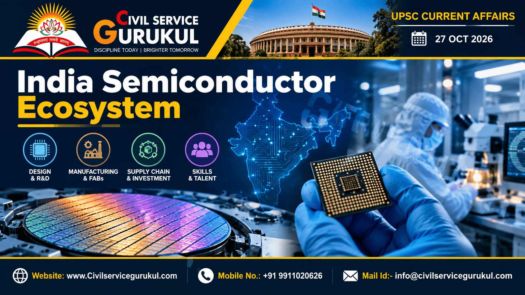
India Semiconductor Mission 2026: Chip Manufacturing, Design, OSAT and India's Technology Future
A comprehensive UPSC analysis of semiconductor fabrication, chip design, assembly, testing, industrial policy, skilled employment and strategic supply-chain resilience.
Published: 27 October 2026
Prepared by: Civil Service Gurukul Research Desk
Semiconductors are essential components in modern electronics, including smartphones, vehicles, communication networks, medical equipment and defence systems.
India's semiconductor strategy seeks to develop capabilities across design, manufacturing, assembly, testing and packaging.
An October 2026 industry discussion highlighted that long-term competitiveness depends not merely on constructing fabrication plants but also on skills, infrastructure, domestic innovation and reliable global partnerships.
GS Paper II: Government policies, industrial development initiatives and institutional coordination.
GS Paper III: Science and technology, industrial growth, investment, employment, economic security and infrastructure.
Prelims: Semiconductors, silicon, fabrication plants, OSAT, ATMP and design incentives.
1. Why Is India's Semiconductor Ecosystem in the News?
An industry discussion highlighted on 26 October 2026 drew attention to India's effort to move from its established chip-design talent base towards a broader semiconductor manufacturing and packaging ecosystem.
The central policy question is whether India can develop a sustainable value chain rather than relying on isolated investment projects.
Semiconductor manufacturing involves substantial capital expenditure, highly specialised technology, advanced infrastructure and international supply-chain coordination.
For UPSC aspirants, the topic connects industrial policy, economic development, technological innovation, employment and national security.
2. What Are Semiconductors?
A semiconductor is a material whose electrical conductivity lies between that of a conductor and an insulator and can be controlled through appropriate physical or chemical processes.
Silicon is one of the most widely used semiconductor materials.
Why are semiconductors important?
- They enable electronic processing and control.
- They support communication and computing systems.
- They are used in vehicles and industrial equipment.
- They are essential for many medical and defence technologies.
- They underpin modern digital infrastructure.
A disruption in semiconductor supply can therefore affect several industries simultaneously.
3. India Semiconductor Mission
The India Semiconductor Mission supports the development of India's semiconductor and display manufacturing ecosystem.
The policy framework includes support for eligible semiconductor fabrication, compound semiconductor, assembly and packaging, and chip-design activities.
Important policy instruments
- Fiscal support for eligible semiconductor manufacturing projects.
- Support for semiconductor packaging and testing capabilities.
- Design Linked Incentive measures for domestic chip-design activity.
- Efforts to attract investment and develop industrial capabilities.
The mission's scheme framework has provided support of up to 50% of project cost for certain eligible fabrication projects, subject to applicable conditions.
However, fiscal incentives alone cannot ensure commercial viability.
4. Understanding the Semiconductor Value Chain
The semiconductor value chain includes multiple specialised activities.
| Stage | Key Activity |
|---|---|
| Chip Design | Developing circuit architecture and functionality |
| Wafer Fabrication | Manufacturing integrated circuits on semiconductor wafers |
| Assembly | Preparing fabricated chips for practical use |
| Testing | Checking performance and reliability |
| Packaging | Protecting chips and enabling electrical connections |
What is a semiconductor fab?
A fabrication plant, commonly called a fab, manufactures integrated circuits on semiconductor wafers using highly precise processes.
What is OSAT?
OSAT stands for Outsourced Semiconductor Assembly and Test.
What is ATMP?
ATMP stands for Assembly, Testing, Marking and Packaging.
OSAT and ATMP activities are associated with back-end semiconductor manufacturing.
5. Chip Design, Innovation and Domestic Intellectual Property
India possesses a substantial base of engineering and chip-design talent.
However, the presence of design professionals does not automatically translate into ownership of commercially valuable domestic semiconductor intellectual property.
Support required by design start-ups
- Affordable electronic-design automation tools.
- Access to prototyping facilities.
- Testing and validation support.
- Research collaboration with universities.
- Customer access and procurement opportunities.
- Support for commercialisation of intellectual property.
Strengthening domestic design capabilities can improve India's position within global semiconductor value chains.
6. Infrastructure Requirements for Chip Manufacturing
Semiconductor fabrication requires exceptionally reliable infrastructure and sophisticated manufacturing conditions.
Critical requirements
- Reliable electricity supply.
- Ultrapure water systems.
- Specialised chemicals and gases.
- Advanced manufacturing equipment.
- Cleanroom environments.
- Highly skilled technicians and engineers.
- Effective environmental safeguards.
These requirements explain why semiconductor projects involve high entry barriers and long investment horizons.
Industrial policy must therefore combine incentives with utilities, logistics, supplier development and workforce preparation.
7. Strategic and Economic Importance for India
Economic development
A competitive semiconductor ecosystem can support advanced manufacturing, investment, technological upgrading and specialised employment.
Supply-chain resilience
Domestic capabilities and diversified international partnerships can reduce exposure to disruptions in critical electronic components.
Strategic autonomy
Semiconductors are important inputs for communication, defence, industrial automation and digital infrastructure.
Greater domestic capability can strengthen resilience, although complete self-sufficiency may not be economically practical.
Skilled employment
The sector requires engineers, technicians, equipment specialists, quality-control professionals and manufacturing support workers.
8. Major Challenges and Policy Trade-offs
| Challenge | Policy Consideration |
|---|---|
| High Capital Costs | Transparent and performance-linked fiscal support |
| Technology Dependence | Research, partnerships and domestic capability development |
| Water and Energy Demand | Reliable utilities and environmental planning |
| Specialised Skill Gaps | University and vocational training |
| Global Supply Dependence | Diversification and trusted partnerships |
| Commercial Uncertainty | Customer access, quality assurance and realistic timelines |
A successful semiconductor strategy must balance national ambition with financial discipline, technological feasibility and environmental sustainability.
9. Way Forward: Building a Competitive Semiconductor Ecosystem
- Link incentives to verifiable production and employment milestones.
- Expand semiconductor laboratories in universities and technical institutions.
- Develop technician training and specialised vocational programmes.
- Support domestic chip-design start-ups and prototyping access.
- Strengthen supplier clusters and industrial infrastructure.
- Promote water recycling and efficient energy use.
- Develop trusted international technology partnerships.
- Encourage transparent monitoring of publicly supported projects.
10. UPSC Prelims Quick Revision
| Term | Important Fact |
|---|---|
| Semiconductor | Material with controllable electrical conductivity |
| Silicon | Common semiconductor material |
| Fab | Semiconductor wafer fabrication facility |
| OSAT | Outsourced Semiconductor Assembly and Test |
| ATMP | Assembly, Testing, Marking and Packaging |
| DLI | Design Linked Incentive |
| India Semiconductor Mission | Supports important semiconductor ecosystem initiatives |
11. UPSC Prelims Practice MCQs
Which activity is most closely associated with OSAT?
- Mining all rare earths used in chips.
- Outsourced chip assembly and testing.
- Drafting the Constitution.
- Broadcasting satellite television.
OSAT refers to Outsourced Semiconductor Assembly and Test, a distinct part of the semiconductor value chain.
Consider the following statements:
- Silicon is commonly used in semiconductor manufacturing.
- Semiconductor conductivity can be controlled through doping.
- OSAT refers primarily to wafer fabrication.
Which statements are correct?
- 1 and 2 only
- 2 and 3 only
- 1 and 3 only
- 1, 2 and 3
Statements 1 and 2 are correct. OSAT concerns assembly and testing rather than wafer fabrication.
The Design Linked Incentive scheme is primarily associated with:
- Development of semiconductor design capabilities.
- Regulation of agricultural markets.
- Construction of national highways.
- Expansion of railway passenger services.
The Design Linked Incentive framework supports semiconductor design activity and related domestic intellectual property development.
Which of the following are important requirements for semiconductor fabrication?
- Reliable electricity.
- Ultrapure water.
- Specialised equipment.
- Skilled technical personnel.
Select the correct answer:
- 1 and 2 only
- 2, 3 and 4 only
- 1, 3 and 4 only
- 1, 2, 3 and 4
All four are important inputs for semiconductor fabrication facilities.
12. UPSC Mains Practice Questions
Assess India's opportunities and constraints in developing a resilient semiconductor ecosystem.
Suggested Answer Framework:
- Explain the strategic significance of semiconductors.
- Describe the global semiconductor value chain.
- Identify India's design talent and policy support.
- Discuss capital, infrastructure and technology constraints.
- Recommend measurable and internationally integrated policy.
"Semiconductor competitiveness depends on an ecosystem rather than isolated manufacturing plants." Discuss.
Suggested Answer Framework:
- Explain the stages of chip production.
- Discuss fabrication, packaging and testing.
- Analyse skilled labour and infrastructure needs.
- Examine domestic design and supplier capabilities.
- Conclude with integrated industrial development.
Examine the role of fiscal incentives, technology partnerships and human-capital development in India's semiconductor strategy.
Suggested Answer Framework:
- Introduce the India Semiconductor Mission.
- Discuss high entry barriers.
- Explain the benefits and risks of subsidies.
- Evaluate technology transfer and skill development.
- Recommend transparent, performance-based support.
13. Frequently Asked Questions
What is the India Semiconductor Mission?
It is an initiative supporting the development of semiconductor and related manufacturing and design capabilities in India.
What is a semiconductor fab?
A fab is a facility that manufactures integrated circuits on semiconductor wafers.
Is chip design the same as fabrication?
No. Chip design develops circuit architecture, while fabrication manufactures the circuits on wafers.
What is OSAT?
OSAT stands for Outsourced Semiconductor Assembly and Test.
What is ATMP?
ATMP stands for Assembly, Testing, Marking and Packaging.
Does a government subsidy guarantee successful chip production?
No. Commercial success also depends on technology, infrastructure, customers, product quality and execution.
Why is semiconductor manufacturing important for UPSC?
It connects industrial policy, technological development, employment, economic security, supply-chain resilience and strategic autonomy.
14. Conclusion
India's semiconductor strategy represents an effort to strengthen technological capability, industrial competitiveness and economic resilience.
However, semiconductor development requires more than financial incentives or the construction of fabrication facilities.
For UPSC aspirants, the central lesson is that long-term semiconductor leadership depends on integrated progress across design, manufacturing, packaging, skills, infrastructure and global market participation.
Editorial Note: This is an original educational explainer based on the supplied October 2026 article. Project-specific investment, approval and production figures should be checked against current official announcements before publication. It is not an official UPSC or government notice.
Prepare with Mentors Who Cleared the Exam
Get personalized study plans, evaluated answer models, and test series access.